Part 2 – How does flash memory work?

The heart of any SD Card is the flash memory chip. Hence to understand why SD Card quality is not always the same we need to know how flash memory is manufactured and how it works.
This post is part of a three part mini series about SD Cards with some in depth information.
- Part 1 – How to classify SD Cards and choose the right Card for an application
- Part 2 – How does flash memory work
- Part 3 – What are Card grades and why are they important
Content
- Why Silicon is used to create flash memory
- Silicon Wafer Production
- Production of Dies
- Flash Memory Structure
- Reading and Writing Data
If you need an overview or a quick reminder on the topic, this info graphic should serve you well.
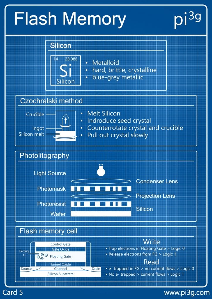
Why Silicon is used to create flash memory
Flash memory and other micro chips are made out of silicon because it is a semiconductor. That means that it is only conducting electricity under certain conditions. Besides that, silicon is the second most abundant element in the earth’s crust.
The semiconductivity of silicon grants manufacturers complete control over the electrical properties of silicon based materials by adding tiny amounts of impurities. These are mostly boron, phosphorus, arsenic and antimony.
Silicon Wafer Production
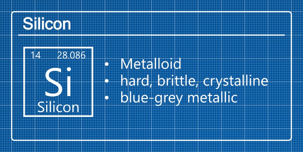
The first step in the production of flash memory is to create a silicon ingot. There are several methods to obtain a cylindrical ingot. Let us have a look at the commonly used Czochralski method.
Czochralski method
The Polish chemist Jan Czochralski invented a method to produce monocrystalline silicon ingots of high purity.
Silicon is molten in a crucible. After that a seed crystal is introduced into the melt. It is slowly pulled upwards, while the crucible and the crystal rotate in opposite directions. This leads to a very homogeneous cylindrical ingot of silicon, which is also called a boule.
Slicing
A wafer saw slices the boule into wafers, which are very thin discs (about 100–500 μm thick). The wafers are physically and chemically polished to remove any defects and impurities up to an atomic scale.
Production of Dies
Of course the wafers possess no super powers yet. They first have to be turned into dies. A die is just a piece of silicon that contains an Integrated Circuit.
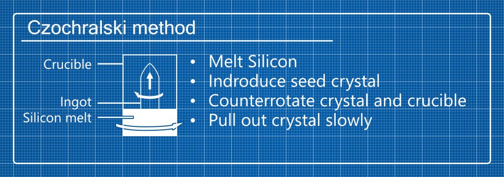
The most commonly used process to print the Integrated Circuit onto the wafer is photolitography.
This process is simple to understand but very difficult to perform with consistent quality, due to the icredibly small scale of Integrated Circuits.
Photolitography
Take a look at the graphic below, which shows the Photolitography setup.
The wafer is cleaned again after shipping to remove any contaminants originating from the packaging. Then it is primed with a microscopicly thin and perfectly even layer of silicon and photoresist. An aperture consisting of a light source and lenses projects the photomask onto the wafer. Most companies use high energy UV light. After some additional steps the pattern from the photomask is transferred onto the silicon layer on top of the wafer.
After that, the first layer must be cleaned to be able to start with the next layer. The photolitography machine repeats these steps for each layer until the specific 3D structure of the flash memory is finished.
At this stage the wafer looks like a disc with lots of cells on top. These mostly quadratic cells are the individual dies, which are single units of flash memory in this case.
Before the wafers can be processed further, the quality of each die needs to be determined. The result is a so called wafer map that indicates the grade of each die on the wafer. Due to the nature of the production process there is a tendency that in the center perform better than dies near the edge.
The dies that reach the required quality standard are the cut out of the wafer and built into flash memory devices.
Now you know how flash memory is produced. Of course it is nearly impossible to have perfectly consistent results every time because of the giant amount of paramters that influence the production.
Everything from the materials to the machines has to be of perfect quality to maximise the amounts of functioning dies on each wafer.
Flash Memory Structure
A single flash memory cell can store 1 Bit. The cell consists of a source and a drain as well as a floating gate and a control gate all on top of the silicon substrate.

There are oxide layers between the control gate, the floating gate and the silicon substrate. They prevent electrons from moving freely but electrons can tunnel through these layers under certain circumstances.
Reading and Writing Data
Writing and reading operations are controlled by applying voltages to the flash memory cell.
Reading
To read the stored Bit, the source is pulled to ground or 0V and around 3V are applied to the drain and control gate. This forces the electrons to move horizontally from the source to the drain if the floating gate is empty. The flow of current is interpreted as a logic 1.
However if electrons are trapped in the floating gate they prevent the flow of current from the source to the drain, which is interpreted as a logic 0.
Writing
To write a logic 0 to the flash memory cell electrons need to be trapped in the floating gate. This is achieved by appling 0V to the source, around 7V to the drain and an even higher voltage of around 10V to the control gate.
The electrons are forced to move horizontally from the source to the drain again but some will tunnel into the floating gate because of the higher voltage. Once the voltages are removed, these electrons are trapped between the two oxide layers for up to 10 years! But eventually they will tunnel out of the floating gate and the data will be lost. Hence you should make regular backups of any important files residing on flash drives.
To remove the electrons from the floating gate and write a logic 1 the control gate is pulled to ground or 0V and the source, silicon substrate and drain are put on around 10V. That way the electrons are forced out of the floating gate.
Of course each flash memory cell has a limited number of read and write operations until it wears out. Hence most modern systems try to distribute data so that no cell is used more often than others, to ensure maximum lifespan of the flash memory.
Conclusion
So now that you’ve become a master of flash memory, be sure to check out the third installment in this series: What are Card grades and why are they important?
And, in the meantime, if you’re looking to buy an SD card, you can get one from our sister company, buyzero.de.
[…] How does Flash Memory work? […]